Today, Lawrence Livermore National Lab (LLNL) and IBM announce the development of a new Scale-up Synaptic Supercomputer (NS16e) that highly integrates 16 TrueNorth Chips in a 4×4 array to deliver 16 million neurons and 256 million synapses. LLNL will also receive an end-to-end software ecosystem that consists of a simulator; a programming language; an integrated programming environment; a library of algorithms as well as applications; firmware; tools for composing neural networks for deep learning; a teaching curriculum; and cloud enablement. Also, don’t miss the story in The Wall Street Journal (sign-in required) and the perspective and a video by LLNL’s Brian Van Essen.
To provide insights into what it took to achieve this significant milestone in the history of our project, following are four intertwined perspectives from my colleagues:
- Filipp Akopyan — First Steps to an Efficient Scalable NeuroSynaptic Supercomputer.
- Bill Risk and Ben Shaw — Creating an Iconic Enclosure for the NS16e.
- Jun Sawada — NS16e System as a Neural Network Development Workstation.
- Brian Taba — How to Program a Synaptic Supercomputer.
The following timeline provides context for today’s milestone in terms of the continued evolution of our project.

Illustration Credit: William Risk

First Steps to an Efficient Scalable NeuroSynaptic Supercomputer
Guest Blog by Filipp Akopyan
Recently, IBM’s Brain-inspired Computing Team has revealed the world’s first 1 million-neuron evaluation platform for mobile applications (NS1e), based on IBM’s TrueNorth (TN) neurosynaptic chip. Afterwards, we demonstrated the first 16 million-neuron scale-out system (NS1e-16) assembled using 16 instances of the NS1e board along with supporting periphery, which includes a host server, network router, power supervisors, and other components. Detailed Information on NS1e-16 may be found at [Revealed: A Scale-Out Synaptic Supercomputer (NS1e-16)].
NS1e-16 is a powerful system, but we needed a bigger challenge. Why not build a more compact, more efficient 16 million neuron system that can fit in your shoe box?! We have had some initial prototypes of such a system before, but nothing that could actually be delivered to our customers and partners. So, with the support of LLNL, we embarked on a journey to NeuroSynaptic 16 million-neuron evaluation platform, NS16e (note the subtle but significant lettering difference from the earlier NS1e-16 system).
NS16e evaluation platform consists of the following main components: a custom 4×4 board, a custom Interposer board, and an Avnet off-the-shelf Zynq SOC mini module, AES-MMP-7Z045-G. The three boards are assembled into a single NS16e structure using vertical stacking/mating connectors to supply power to all the boards and to exchange data and control signals.
The 4×4 board contains 16 programmable TrueNorth chips capable of implementing large-scale (up to 16 million neurons) neural models for various applications. Each TrueNorth neurosynaptic chip has 4092 usable cores with each core containing 256 neurons, 256 axons, and 65536 synapses. To maximize the communication bandwidth with the TrueNorth chips on the 4×4 board, we use data port expanders, which access the TrueNorth input/output ports. A similar set of IC-s is used to perform the configuration of all the TrueNorth chips using scan chains. The 4×4 board also hosts all the TrueNorth power domain regulators, power supervisor, current sensing circuitry and several SPI/I2C programmable devices.
The Interposer board provides high speed interfaces and power domains for all the NS16e system components. It contains a PCIe x4 connector for high-speed communication with a host machine and an SFP+ Ethernet cage (which is not currently enabled). The Interposer also contains a power supervisor and a series of electronic fuses (along with the 4×4 board) meant to shut down the system in case of a power failure. For debugging purposes the Interposer board (as well as the 4×4 board) contains LED-s, which may indicate failures on power domains. The Interposer also hosts a JTAG connector for programing the Zynq module.
The Zynq module provides an FPGA fabric for implementing custom glue logic to control and potential modify (if there is such a requirement) the incoming/outgoing data to and from NS16e. Specifically, the Zynq fabric may be used for DMA, data-to-spike transduction, filtering, etc. The high speed transceivers on the SOC (system-on-chip) are used to provide a PCIe communication bridge between NS16e and the host system. The Zynq SOC also contains two ARM processor cores, which are not enabled on the current revision of NS16e to minimize power consumption.
The team created a specification, schematics and performed the physical design (layout) of the system. We have then manufactured the boards and assembled them using the latest cutting-edge electronic components.
So without further ado, we present to you the first NS16e prototype system. Figure 1 shows the assembled 4×4 board (no chips); Figure 2 shows the assembled Interposer board.
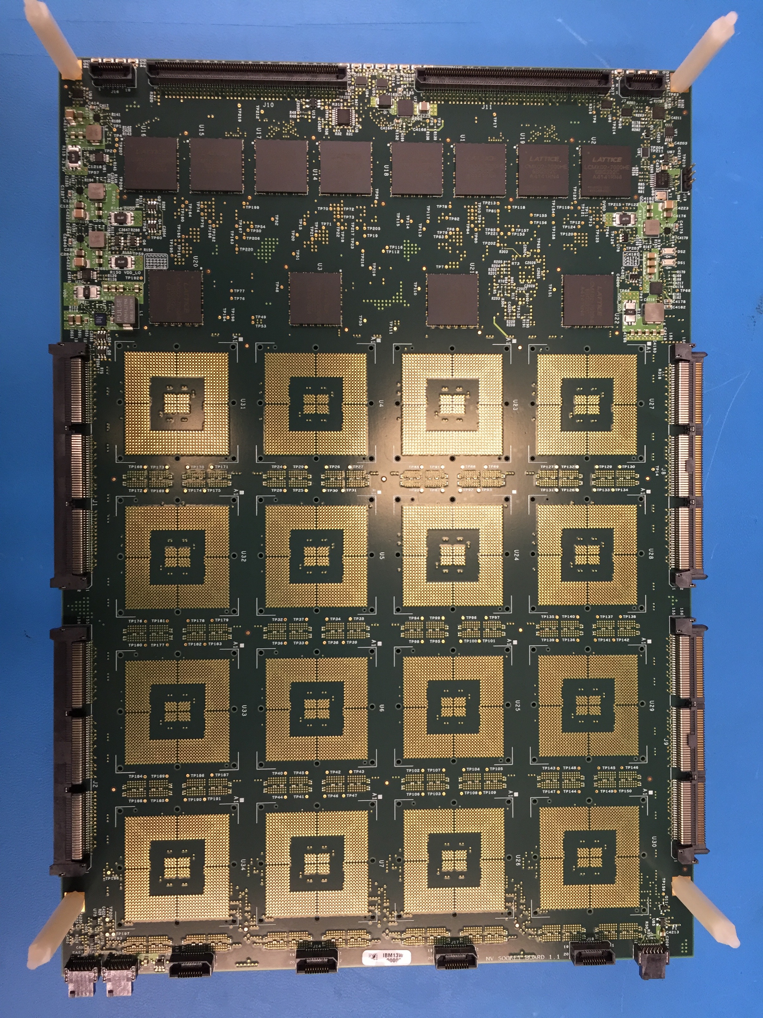
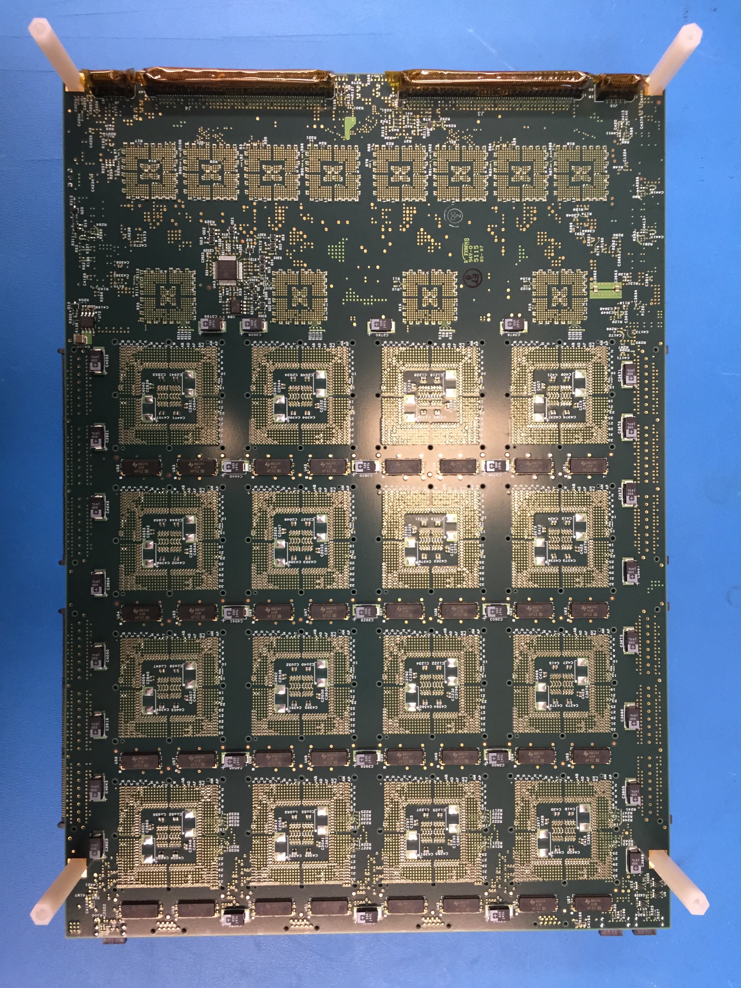
Figure 1. NS16e: 4×4 board TOP on the left, and BOTTOM on the right.

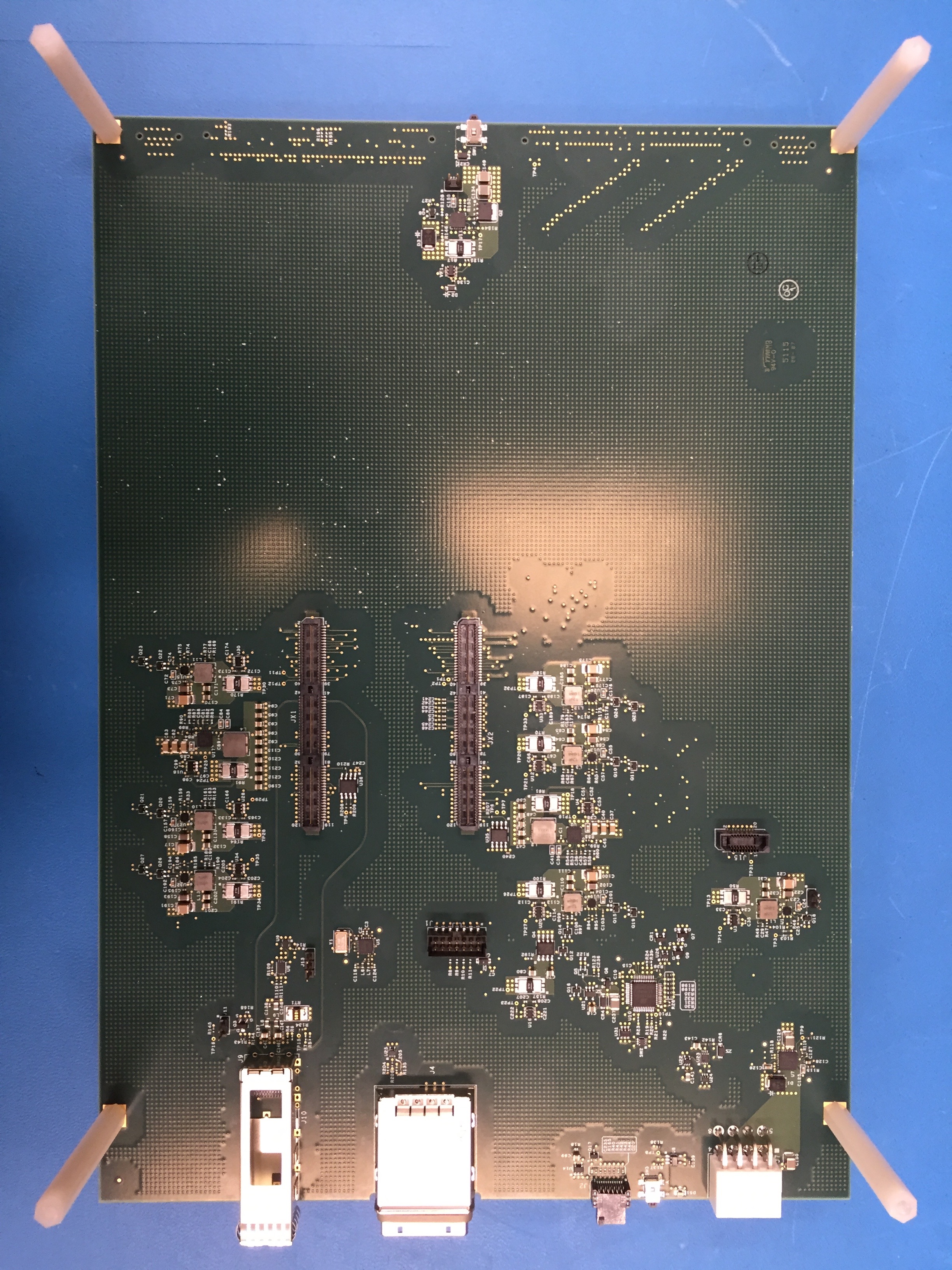
Figure 2. NS16e: Interposer board TOP on the left, and BOTTOM on the right.
Since the current number of TrueNorth chips is limited, we have decided to use an assembly risk aversion technique and populate the initial few systems without soldering down the TrueNorth chips. This gives us an opportunity to test the complete design of the system up to (but not including) the actual TrueNorth chips. Figure 3 shows the two boards side-by-side, ready for stacking on top of one another (Zynq module not depicted).
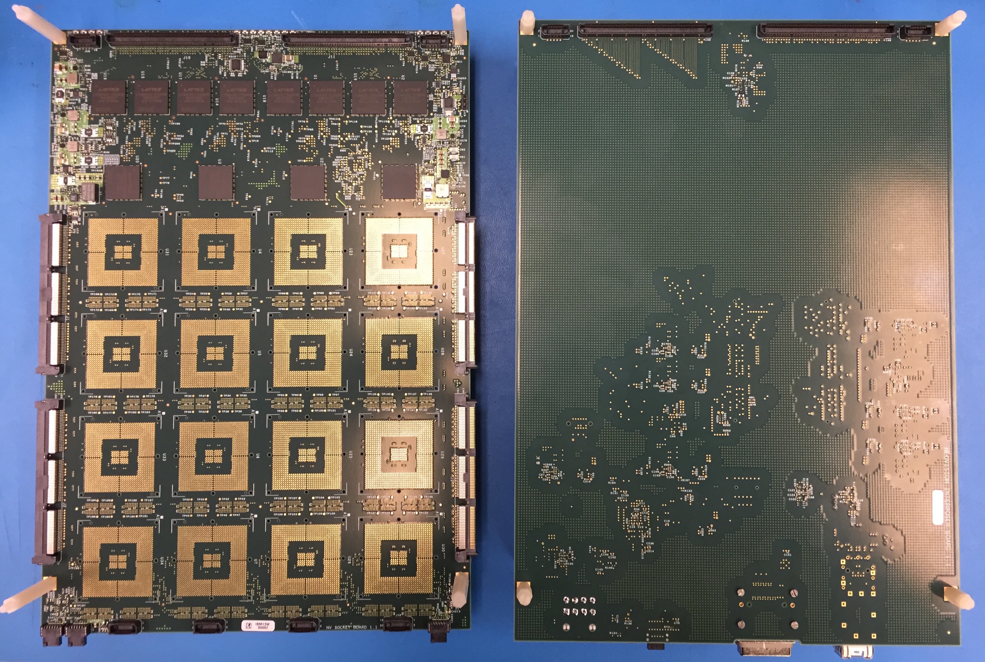
Figure 3. NS16e: 4×4 and Interposer boards side-by-side (ready for mating).
As one can imagine, the bring-up of such an unconventional system is not a trivial task. We have developed and put in place various hardware, firmware and software tests to verify the functionality of the system.
On these first prototypes we have provisioned for special type of sockets, which can be populated post-assembly to host the actual TrueNorth chips. Once we have fully verified the functionality of the two newly designed boards without the chips, we have populated the 4×4 board with TrueNorth chips by the means of aforementioned sockets, as shown in Figure 4.
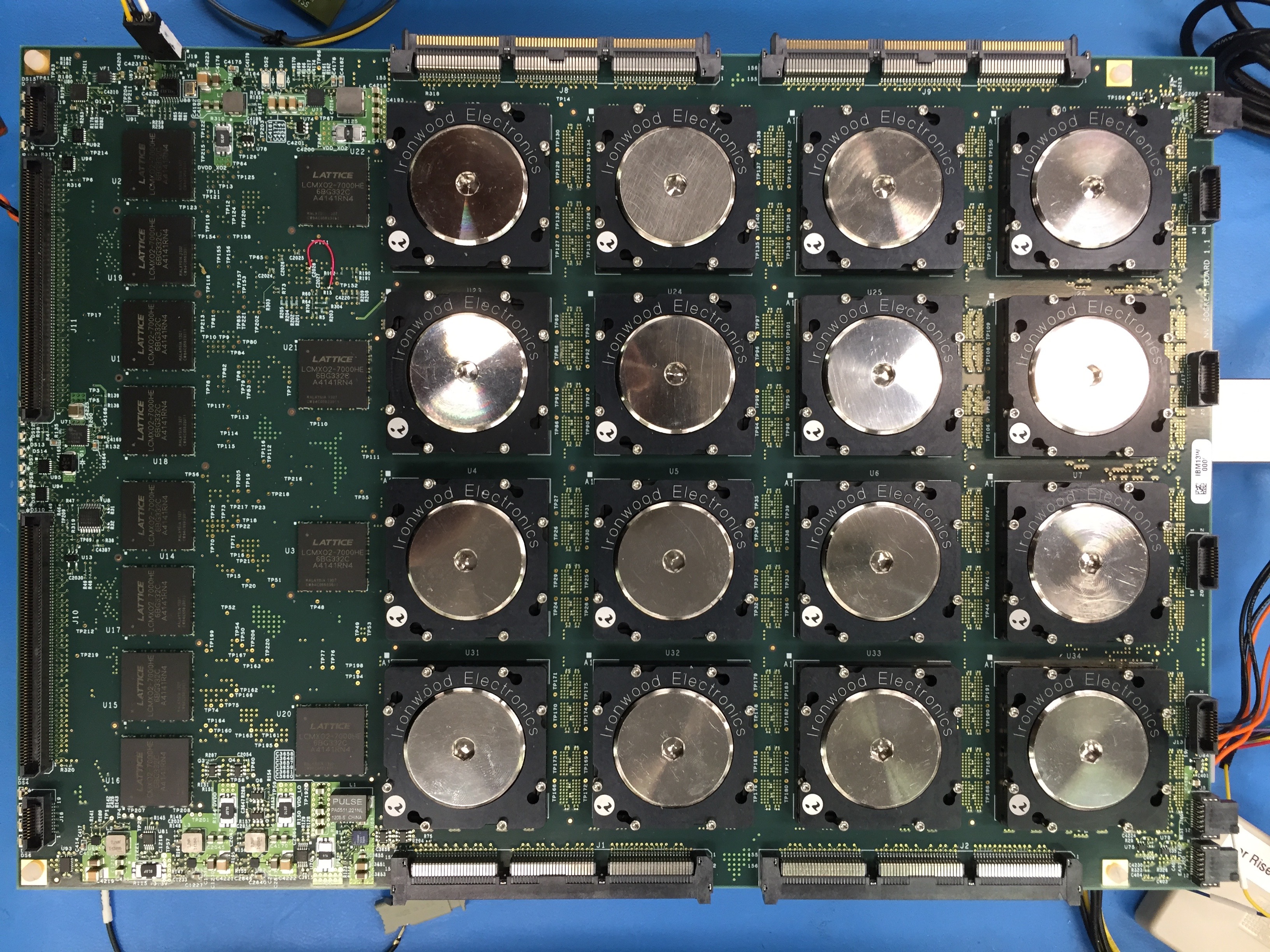
Figure 4. NS16e: System populated with TN-chips using sockets.
Power up of this platform has to be performed by stages with extra care to make sure that the current draw of the system is within reason (i.e. no shorts); all the key interface signals between TrueNorth chips and glue logic are monitored with oscilloscopes for proper operation and signal integrity. The low level bring-up of the full system is depicted in Figure 5.
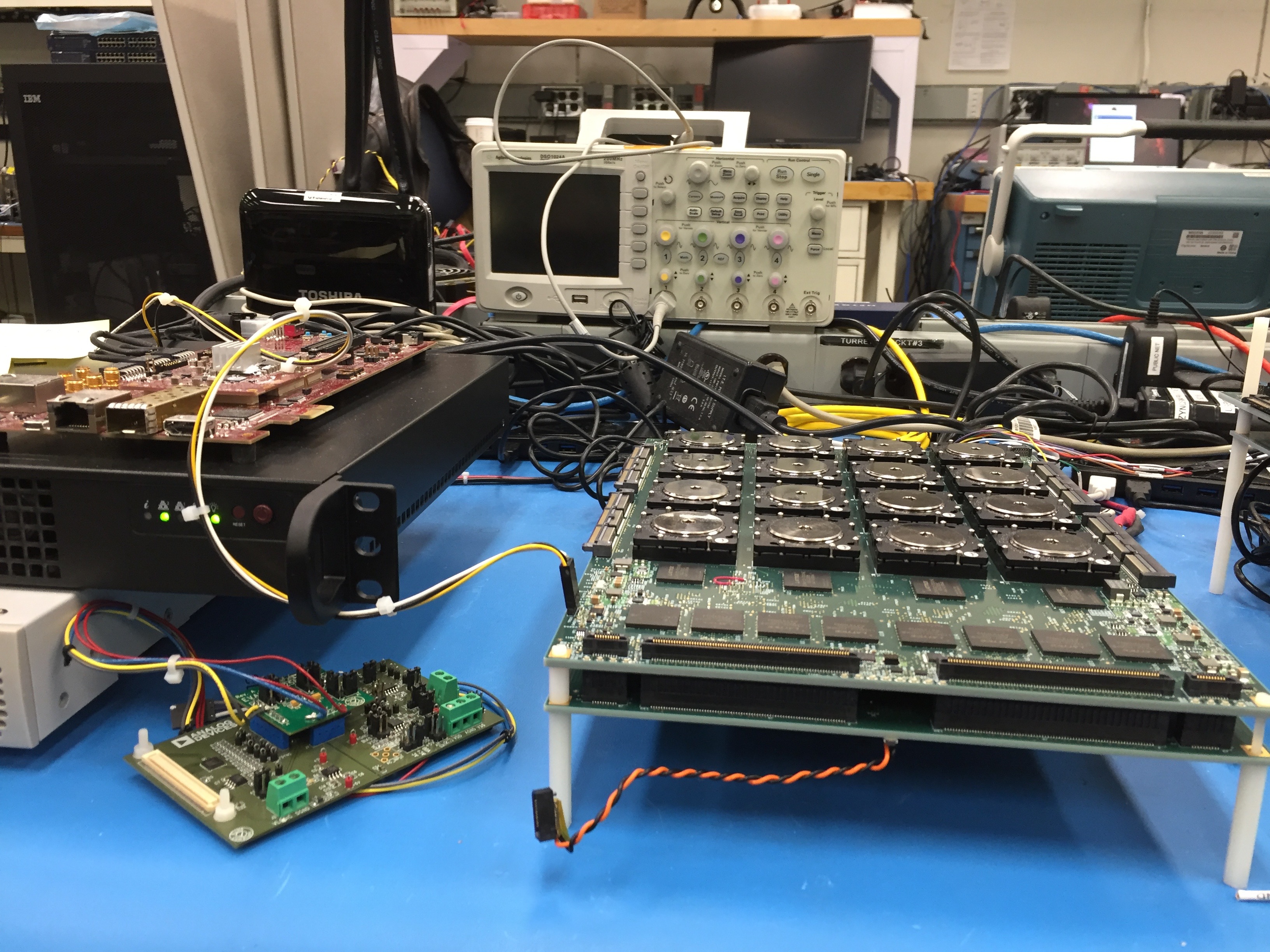
Figure 5. NS16e: Low level bring-up with TN-chips in sockets.
Bringing-up and debugging complex boards takes at least several days (with luck on your side). This platform was no exception. Once we had all the low level tests running correctly on system with sockets, we have given a green light to our board assembler to create the first prototypes with soldered down TrueNorth chips. The first 4×4 with soldered chips is shown in Figure 6.
Figure 6: First 4×4 prototype with soldered down TN-chips.
Now that all the low level tests have been successfully completed, we connect the new NS16e systems to the host servers (Figure 7) using several interfaces: Xilinx JTAG for Zynq programming, Lattice JTAG for power supervisor and FPGA programming, PCIe gen2 link for data exchange between host server and TrueNorth chips.
Figure 7: NS16e systems connected to host machines.
At this point the high level testing takes over and we start running neural network algorithms and applications right on the new NS16e system.
Some of us (myself included) like to work on the weekends, since it is quiet and the janitors don’t bother you when you stay late! Also there are no mandatory meetings, so it is just you and the pure drive to create the world’s most advanced neurosynaptic system! The only problem is that the cafeteria is closed … so we have to get pizza!
Figure 8. Scott Lekuch having a bite to eat and performing NS16e application testing simultaneously.
At the end of this exciting journey we have successfully brought up the NS16e prototypes. Now with the help of our highly-talented software team we can run complex neural applications on this powerful platform. Check out the blogs by Jun Sawada and Brian Taba for the application details. Advanced image/sound recognition and classification in real time on 16 million artificial spiking neurons, anyone?!

Creating an Iconic Enclosure for the NS16e
Guest Blog by Bill Risk and Ben Shaw
For deployment to LLNL, the three-board stack that Filipp Akopyan described above needed to be housed in a protective enclosure. Since the NS16e system is a first-of-its-kind neurosynaptic supercomputer, we wanted to create an interesting, iconic enclosure design that would reflect this novelty, while securing the boards and allowing access to the required connectors, switches, and indicators. Since the board configuration was already fixed, the enclosure had to be designed to accommodate the existing placement of these components and the irregular shape of the three-board stack.
These goals created a challenging design problem, but fortunately, we have been collaborating for several years with the highly creative IBM Design Team, who had previously designed concept models showing potential applications of the TrueNorth chip [Cognitive Apps ]. Aaron Cox (Industrial Design) had worked with us earlier to create an iconic gold cover for the chip (Figure 9). The design of this cover—with tabs in the four cardinal directions—expresses a key feature of the TrueNorth chip: its built-in ability to be tiled with other chips in a two-dimensional array. Since the NS16e is the first system we’ve built that fully exploits this tileability, we wanted to ensure that the enclosure made the chip caps visible, to dramatically highlight the 4×4 array of chips contained in the system (Figure 10). Working on the overall personality of this research prototype system, Camillo Sassano (Industrial Design) and Kevin Schultz (User Experience) created a design that uses sharp angled surfaces to give the enclosure a shape that appears to change with the viewing angle. A 4×4 array of chamfered pockets on the front features and emphasizes the 3D effect of the golden chips caps, and light accents complement the sculptural geometry of the device.
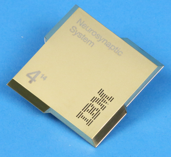
Figure 9. TrueNorth chip cap. The 414 refers
to the number of synapses on a single chip (414=256 million).

Figure 10. NS16e enclosure.
The need to adapt the enclosure to the existing board stack—for example, to actuate pushbutton switches on the edge of one of the PC boards—required the design of some clever mechanisms. A 3D-printed slider provided the ability to press one switch (Figure 11, left panel). In the case of the other pushbutton, a rocker mechanism was used; however, since we also had to provide visual access to an adjacent LED, a light pipe was incorporated into the rocker mechanism, which was 3-D printed in a transparent material to serve both functions (Figure 11, right panel).
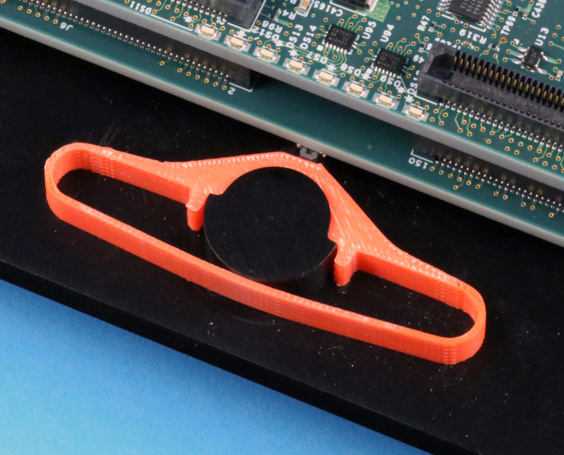
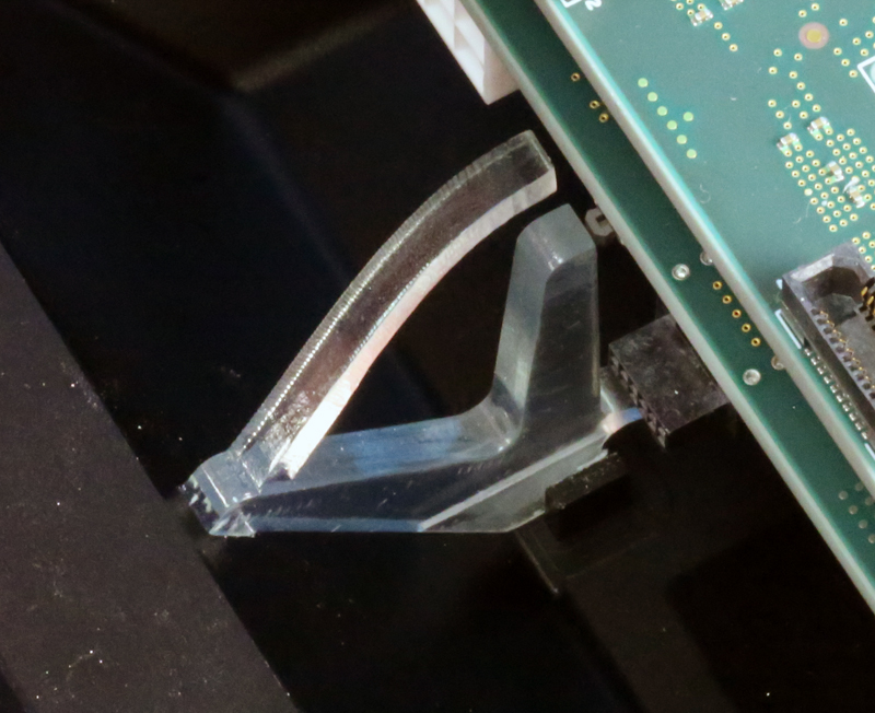
Figure 11. Slide mechanism (left) and rocker mechanism (right).
We wanted the enclosure to support two modes of use: one sitting on a desktop as a standalone unit; the other, placement within a 2U-high drawer for mounting in a server rack. The enclosure was designed so that it could be used in either mode, by attaching either a support foot to allow it to stand on its own (Figure 12) or an adapter that allows it to be mounted in the drawer. In the rackmount mode, the NS16e can be laid flat in the closed drawer for normal operation; the drawer can be opened and the NS16e tilted up for display or maintenance. (Figure 13). Since the enclosure is not visible when the drawer is closed, we added some panel graphics and LED lighting to identify and distinguish the unit.
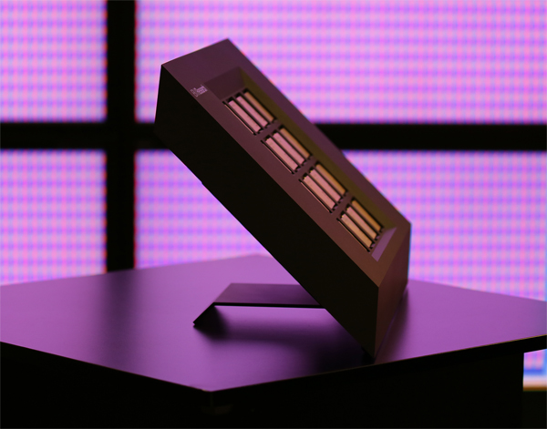
Figure 12. Desktop mode.
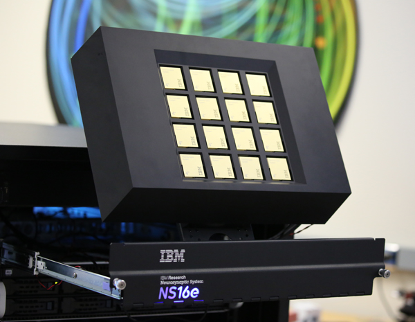
Figure 13. Rackmount mode.
Once mounted in the enclosure, the system is ready for final testing and delivery to LLNL!

NS16e System as a Neural Network Development Workstation
Guest Blog by Jun Sawada
It all started very small, I still remember the first time when we first simulated a single TrueNorth neuron model. It was only on a circuit simulator. A few years later, we have fabricated it into the TrueNorth chip, with 1 million neurons on a stamp-size silicon piece. Today, we have built the NS16e system.
Unlike the scale-out system we built earlier using single-chip boards [Revealed: A Scale-Out Synaptic Supercomputer (NS1e-16)], this machine is intended toward running larger, more powerful neural networks in real time. In a typical setup, the NS16e system is connected to a host x86 server computer by a PCI Express link. The host server can pump large data in and out of the NS16e system. The host server with GPUs can build and train a large neural network, and NS16e can immediately start running it. We can run with a single command the entire end-to-end development process of preprocessing training data, neural network construction, training the network, and optimizing the network for hardware, and running it on the NS16e. Because this development process is very quick on NS16e, NS16e system combined with a powerful host server is a dream machine for large scale neural network development.
In order to tell you how the machine works, please see the system overview in Figure 14. The core neural computation in NS16e takes place in the grid of TrueNorth chips, tiled in an 4×4 grid array. The TrueNorth chip is designed in such a way that, if you connect chip to chip by wires, chips start talking to each other using spikes. All the communication takes place using an asynchronous protocol, without any external clocks or additional interfacing chips.

Figure 14. NS16e system overview.
A host server is connected to NS16e by PCI Express link. It can send and receive 500Mb/sec of data between the NS16e and the host server. The FPGA’s on the NS16e system work like a bridge between the
TrueNorth chips and the host server. In a sense, it is a translator between a conventional von-Neumann computer and a TrueNorth-based neurosynaptic computer, which speak in different languages. A digital von-Neumann computer operates in instructions and binary data, while the neurosynaptic computer talks in neuron spike signals.
When you enter a command to run a neural network model to the host computer, here is what happens. The host computer sends the network model over the PCI Express link, and loads the neural network model to the TrueNorth chips on NS16e. The terminal window on the computer shows the progress of uploading data to NS16e. After 30 seconds or so (depending on the size of the network model), the uploading is completed, and the neural network starts spiking actively. On the host computer screen, you can only see a summary of how many output spikes are generated and how fast all the neurons are updated. Neuron spikes themselves are encoded in a way that is not easy for a person to understand. That is where we use visualizers. It decodes the spikes coming out of NS16e, and visualizes what the NS16e is trying to say.
Let’s say we are going to run an image recognition task on NS16e. We upload the neural network to NS16e, and then we send neuron spikes encoding photo (A) in Figure 15 to NS16e. NS16e produces answers in neuron spikes, and send them back to the visualizer program. The visualizer decodes the spikes and shows picture NS16e chooses like (B) in Figure 15.

Figure 15. Image recognition by NS16e.
The system is still evolving. We continuously create and test new learning algorithms, new model generation techniques, and new optimization algorithms. One unique thing about this machine is that it needs some optimization on how we map the logical representation of a neural network to physical circuits. In our brain, a certain portion of the cortex is responsible for visual recognition and other parts are responsible for motor function. The NS16e has something similar. You may assign which chip is holding which part of a large neural network. For example, we can make each chip to hold a single layer of multi-layer neural network, or we may assign each chip a dissection of the entire multi-layer network corresponding to a patch of an image. This optimization problem, we call “core placement”, is a very unique problem to NS16e-like neurosynaptic machines. This makes some network runs more efficiently and faster, because inter-chip communication is much slower than intra-chip communication. This is one place where we are trying different algorithms and techniques one after another.
The NS16e system is truly a product of great team work. Based on the TrueNorth chip design we worked on in the past, NS16e requires new circuit boards, FPGA programmable logic, system software, placement optimizers, neural network development tools and training algorithms. Only when all of these components start to work together, the whole system begins to produce meaningful answers. It is like creating an entire ecosystem from scratch and integrating them together. We also spent a lot of effort to perfect the system. We have been running countless tests on NS16e and compared the results against our simulation results, in order to make sure that the finished NS16e system has no malfunctioning components. We tracked down every hardware and software issue very earnestly. System testing and documentation team cleaned up many imperfections in our software and documentation. This makes me very proud of the NS16e system, which is a result of diligent work of many people over many years.
At the end of this story, I should say that the NS16e system is just a step forward to much larger scaled systems. Today’s convolutional deep learning network is growing rapidly in size, we would like to build much bigger machines than NS16e. Future scaled-up version of NS16e will certainly run much larger neural network using a fraction of energy consumed by CPUs and GPUs. Perhaps one day we may see a single rack of neurosynaptic system with as many neurons and synapses as in a human brain.

How to Program a Synaptic Supercomputer
Guest Blog by Brian Taba
So how do you actually write programs for a 16-million-neuron synaptic supercomputer? Over the last year, we have built an integrated software ecosystem around a stack of end-to-end TrueNorth development tools. We have bundled this ecosystem into a TrueNorth DevKit for release to partners like LLNL and the many other alumni of last year’s Boot Camp.
Let’s examine one of the reference applications included in our DevKit, a simple TrueNorth image classifier. This example uses a GPU to train a convolutional neural network (CNN) on a standard benchmark dataset, and then deploys the trained network on the NS16e. For more about our algorithm for training CNNs for TrueNorth, see the paper just posted by Steve Esser. Here, we will focus on the developer workflow.
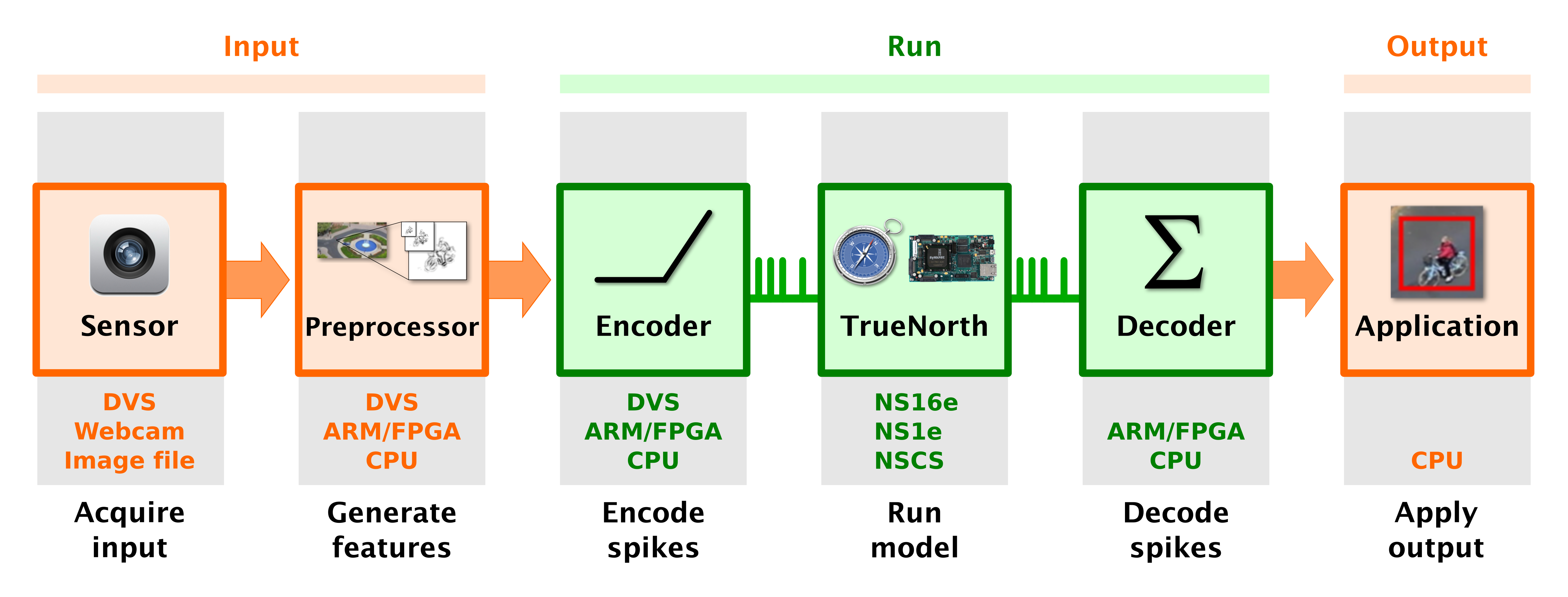
Figure 16. Run flow for a TrueNorth image classifier.
The basic structure of an generic TrueNorth image classifier is laid out in Figure 16. We first acquire a stream of input data, which could be image files read from disk, frames from a webcam, or even natively generated spikes from a Dynamic Vision Sensor (DVS). Raw data might be preprocessed into features like multi-scale edge maps, before being encoded as spike streams for input to TrueNorth. Depending on how the application is distributed across system components, preprocessing and encoding might happen in a server CPU, in the board’s embedded ARM cores or FPGA, or intrinsically in a spiking sensor. Input spikes can be processed by TrueNorth chips on an NS1e or NS16e board, or by the NSCS functional simulator. Finally, output spikes are decoded into classification predictions that are typically sent off-board for visualization.
In this instance, we train a TrueNorth network to classify images from the CIFAR-10 and CIFAR-100 datasets. We simplify the problem by preprocessing and encoding the entire dataset offline. The resulting input spike file is looped through TrueNorth hardware to generate class predictions for the images in the test set, which are streamed to a workstation for visualization.
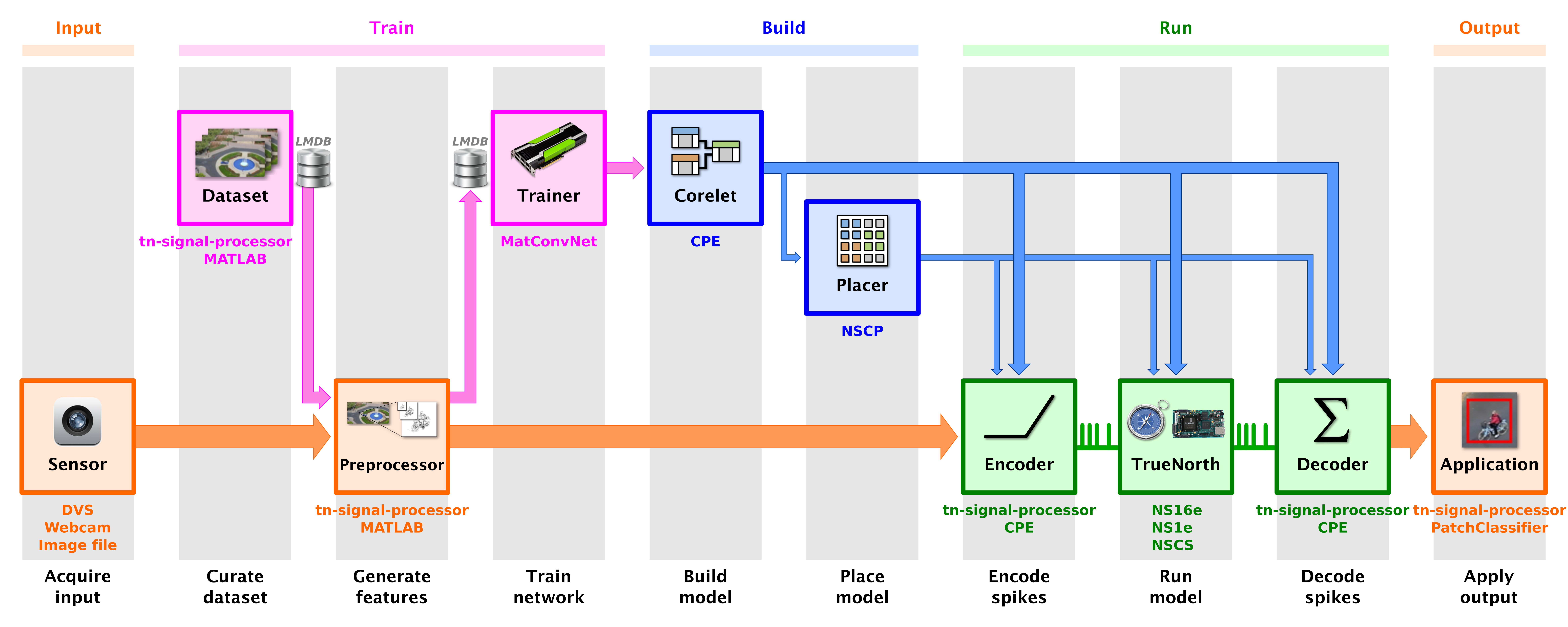
Figure 17. Development flow for a TrueNorth image classifier.
The chain of actions required to train and deploy a TrueNorth image classifier is shown in Figure 17. Out of the box, the DevKit provides at least one tool to fill in every block in this chain, but you can swap out any of our tools for your own, as long as you implement the same interface. For example, the DevKit includes two equivalent tools for reading and writing LMDB databases—a command-line utility called tn-signal-processor, of which more later; or a set of MATLAB MEX files—but as long as the downstream blocks get an LMDB in the right format, they don’t care whether you used one of our tools to make it, or rolled your own.
Dataset/Preprocessor
The first steps in the training workflow are just basic data science. We import the original dataset into a standard format that all of our tools understand, then preprocess it into the features we will use at runtime. We store data in LMDB databases, which are popular for deep learning because their fast read access lets training data pump quickly into a GPU.
To import and preprocess data, we provide a fast C++ command-line utility called tn-signal-processor. Written by David Berg, tn-signal-processor is a Swiss Army knife for manipulating data—it can import JPG and PNG files into our LMDB format, crop, rotate, apply center-surround filters, encode images as spikes, decode spikes into images, visualize data, and more. It can also convert Caffe’s LMDB format to ours and back, so anyone who has already imported their data into Caffe can easily transfer it to the TrueNorth ecosystem, and vice versa.
Trainer/Corelet
Now that we have our data in the proper format, it’s time to train a classifier. TrueNorth Convolutional Networks (TNCN) is a framework for composing and training convolutional neural networks that automatically satisfy the TrueNorth design constraints. Created by Steve Esser using the Corelet Programming Environment (CPE), TNCN frees a data scientist to focus on abstract network properties like layer order, filter size, and data precision; without getting bogged down in the nuts and bolts of how to configure the 23 free parameters in a TrueNorth neuron to represent data as 1-bit spikes instead of 32-bit floats, for example.
TNCN implements high-level classes for common CNN layers like convolution, pooling, dropout, loss, etc. Each layer class has a corresponding corelet that automatically compiles its parameters into legal TrueNorth core configurations. The result is a model file containing a list of logical core parameters that collectively implement the trained TNCN network.
To accelerate training with a GPU, we use a deep learning framework called MatConvNet, which wraps NVIDIA’s cuDNN primitives in binary MEX files that are easy to invoke in MATLAB. MatConvNet is not one of the famous frameworks like Caffe or Torch, but we picked it because we already needed MATLAB for CPE and it’s very convenient to have a single development environment for codesigning TNCN layers and corelets. Of course, when we want to run many training instances in parallel on a GPU cluster, it’s awkward and expensive to activate a MATLAB license on every compute node, so we also provide a compiled version of TNCN that can be run at the command line using the free MATLAB Runtime.
Placer
The final step before deploying this network to hardware is to assign the logical cores in the model file to physical cores in the NS16e chip array. This can be a challenge in multi-chip systems, due to the bandwidth bottleneck at the interface between chips. If cores are sending too many spikes across chip boundaries, spikes might not all arrive at their destinations within the design window of 1 millisecond per simulation tick. Of course, we can always increase the tick period to close timing. But it’s better to reduce cross-chip traffic if possible, by being smarter about where we place cores in the chips.
For the LLNL system, Pallab Datta wrote a new tool from scratch that heuristically places logical cores in the TNCN model file at physical locations in the NS16e core array (Figure 18), based on minimizing chip crossings in the core-to-core connectivity graph. The Neuro Synaptic Core Placer (NSCP) is critical for making large TrueNorth models like a multi-chip TNCN network run successfully in hardware.
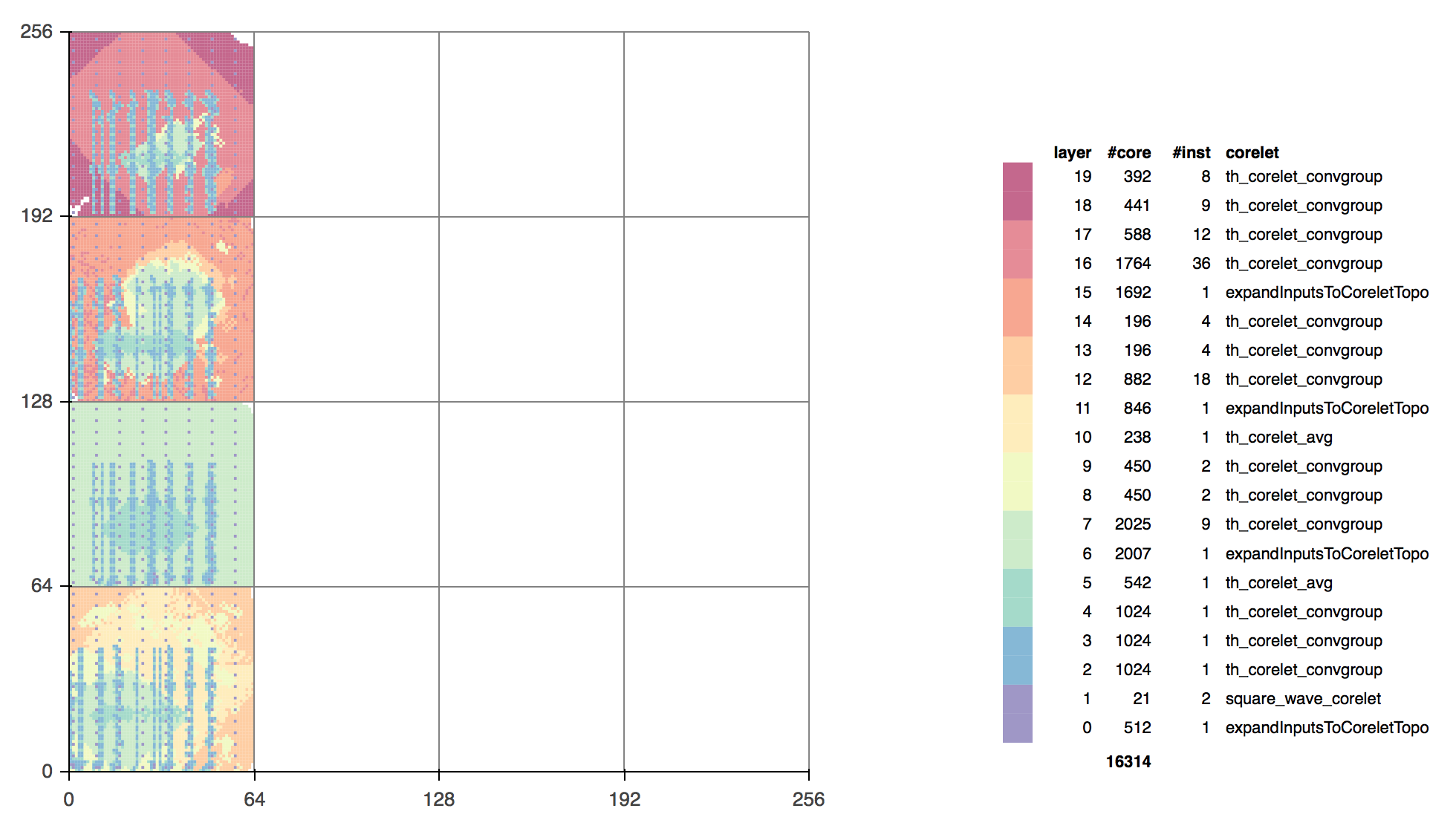
Figure 18. Physical core placement for a 4-chip CIFAR-10 network on NS16e.
Application
Now we can run our trained TrueNorth classifier in hardware, and see it in action! To decode, evaluate, and visualize the test image labels predicted by hardware, we have another command-line utility called PatchClassifier that can be configured to lay out an array of category icons for a given image dataset, with the predicted category outlined in green if correct and red if incorrect. The length of the bar beneath each category indicates the confidence of the classification.
Figure 19 is a screencap of the predicted CIFAR-100 test image classifications being streamed from the NS16e to the PatchClassifier visualizer running on a laptop. In this case, the NS16e correctly classified the test image as a whale (green bar), and its next guess would have been a dolphin (white bar).
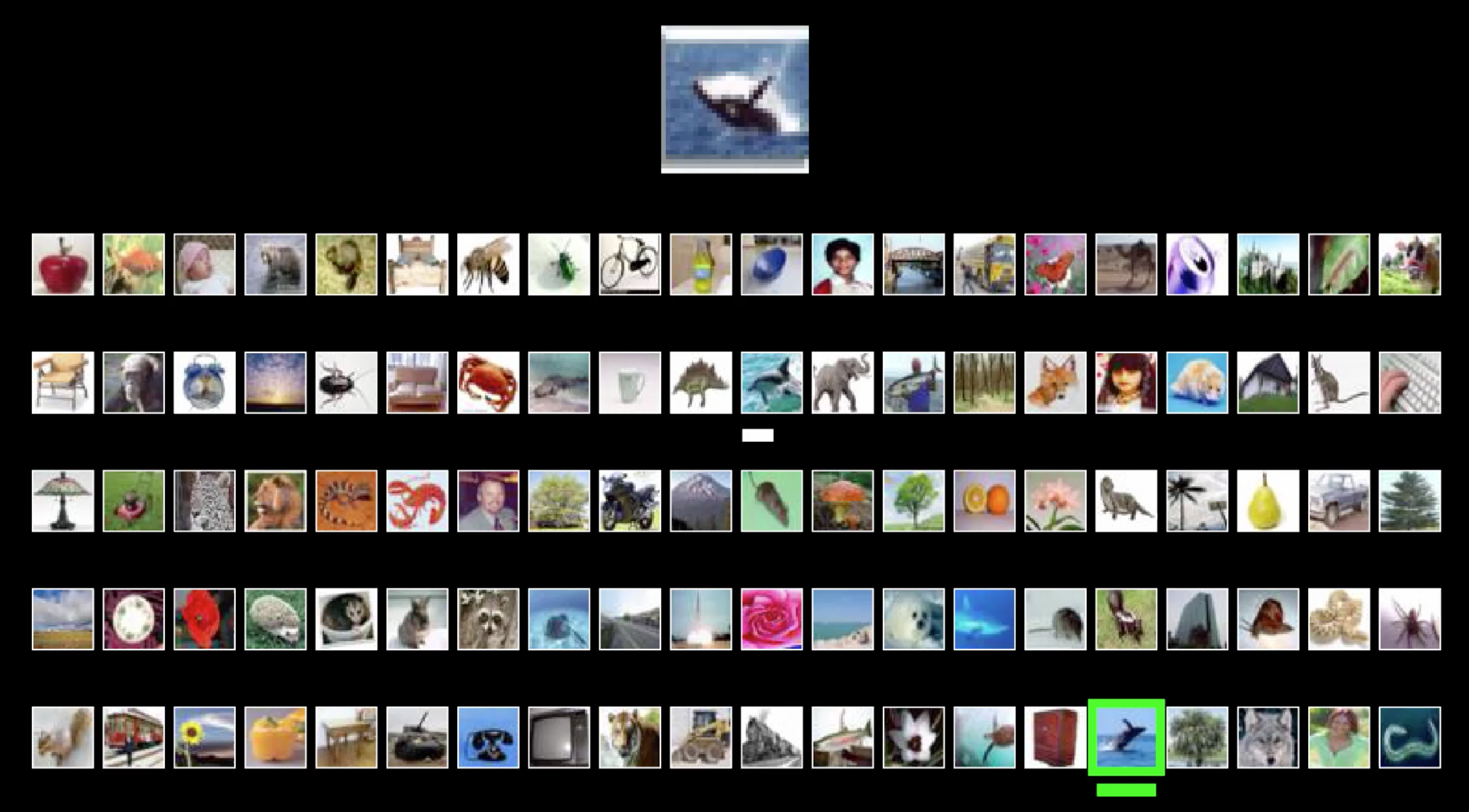
Figure 19. PatchClassifier visualizer configured for CIFAR-100 dataset.